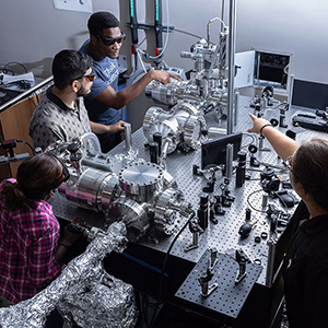
Research Terms
Among the various types of two dimensional (2D) materials, graphene and molybdenum disulfide (MoS2) have received the most attention. Researchers have noted that although graphene has a very high carrier mobility, the lack of a band gap limits its application in nanoelectronic and optical devices. Known for their extraordinary electrical, mechanical, and optical properties, single-layer and few-layer MoS2 sheets have recently received significant attention due to a tunable band gap that ranges from 1.2 eV in bulk layers to 1.8 eV in a single layer.
Noteworthy progress has been made in the modification and the controlling of the essential properties of MoS2. Specifically, modulating the electronic and optical properties further widens the applications of 2D MoS2 and may open up a new era in solid-state electronics and optoelectronics. However, this is challenging because it requires controlably tuning the material's properties.
Advantages
UCF researchers have been able to answer this challenge with a novel plasma-based processing method. This technique, via an external control, continuously tunes the electrical properties of few layers MoS2 flake from semiconducting to insulating, increasing electrical resistivity to more than 1000 times and can potentially be utilized in various device applications such as sensors, diodes, and quantum tunneling devices.
Technical Details
The 2D TMDC material is a layer that is one to eight atomic layers thick (0.9 - 6 nanometers), and the plasma in an oxygen-containing ambient treatment selectively oxidizes to form defect regions in all layers. A single-layer or a few-layer 2D semiconductor transition metal dichalcogenide (TMDC) material is deposited onto a substrate. The energized oxygen molecules interact with MoS2 to create insulating, MoO3-rich, defect regions. This method forms oxidized dielectric TMDC material which has a higher electrical resistivity, compared to untreated material.