Home
About Us
FAQ
Contact Us
Media Tools
ExpertConnect App
MyExpertNet
University Partners
Becoming a Partner
Key Organizations
Search Assistance
Help
Expert Profile
Views:
86
Share
QR code
Edit Profile
Fan Ren
Professor
EG-CHEMICAL ENGINEERING | COLLEGE-ENGINEERING
View:
Select
All (all in one)
Research Terms and Keywords
Publications
Stories
Co-Investigator Network
Websites
Contact
All
Research
Publications
Stories
Network
Websites
Contact
Research Terms & Keywords
Research Terms
Chemical Engineering
Research Projects
Ends
Title
06-2027
BRAIN AND SPINAL CORD INJURY RESEARCH-BSCIP
BRAIN AND SPINAL CORD INJURY RESEARCH-BSCIP
06-2023
Impact Ionization Coefficients in Ga2O3
Impact Ionization Coefficients in Ga2O3
06-2023
OR-DRPD-ROF2019: Rapid Detection of Cerebrospinal Fluid and Development of a Modular Point of Care Testing Solution with Low-Cost Disposable Testing Strips
OR-DRPD-ROF2019: Rapid Detection of Cerebrospinal Fluid and Development of a Modular Point of Care Testing Solution with Low-Cost Disposable Testing Strips
02-2023
Risk factors associated with the prevalence of Peri-Implantitis disease
Risk factors associated with the prevalence of Peri-Implantitis disease
04-2022
Analytical specificity of COVID-19 biosensor
Analytical specificity of COVID-19 biosensor
12-2021
Interaction of Ionizing Radiation in Materials Universit
Interaction of Ionizing Radiation in Materials Universit
09-2021
Novel coatings to minimize surface degradation and fracture susceptibility of dental ceramics
Novel coatings to minimize surface degradation and fracture susceptibility of dental ceramics
08-2021
MIST - Industry Memberships
MIST - Industry Memberships
03-2021
Center of Excellence - Center for Nano-Biosensors
Center of Excellence - Center for Nano-Biosensors
12-2020
Fundamental Studies and Modeling of Radiation Effects in ?-Ga2O3
Fundamental Studies and Modeling of Radiation Effects in ?-Ga2O3
09-2020
Mobile Manipulation and Survey System for H-Canyon and other Applications across the DOE Complex
Mobile Manipulation and Survey System for H-Canyon and other Applications across the DOE Complex
06-2020
LUCENT UNRESTRICTED
LUCENT UNRESTRICTED
05-2019
OR-DRPD-ROF2016:Novel coating to minimize bacterial adhesions and tooth wear in denture acrylic
OR-DRPD-ROF2016:Novel coating to minimize bacterial adhesions and tooth wear in denture acrylic
12-2017
Training for fabrication and design of nitrite based transistors and circuits
Training for fabrication and design of nitrite based transistors and circuits
01-2017
Fundamental Studies and Modeling of Radiation Effects in
Fundamental Studies and Modeling of Radiation Effects in
03-2016
Space Qualifiable Radiation Hardened Compound Semiconduc
Space Qualifiable Radiation Hardened Compound Semiconduc
01-2016
Novel high electron mobility transistor design to lower
Novel high electron mobility transistor design to lower
12-2015
Development of high transparent oxide-based materials
Development of high transparent oxide-based materials
03-2015
Manufacturing Improvements of AlN for Wide Bandgap Semic
Manufacturing Improvements of AlN for Wide Bandgap Semic
08-2013
Vibration-Insensitive and Large-Range MEMS Scanning Four
Vibration-Insensitive and Large-Range MEMS Scanning Four
08-2013
A 21st Century Approach to Electronic Device Reliability
A 21st Century Approach to Electronic Device Reliability
09-2012
AlN/GaN High Electron Mobility Transistor Based THz Emit
AlN/GaN High Electron Mobility Transistor Based THz Emit
04-2012
Development and Fabrication of Nanoelectronic Devices an
Development and Fabrication of Nanoelectronic Devices an
01-2012
Low Cost, Scalable Manufacturing of Surface-Engineered S
Low Cost, Scalable Manufacturing of Surface-Engineered S
07-2011
AIN/GaN HEMT device life time and reliability testing
AIN/GaN HEMT device life time and reliability testing
03-2011
Low Cost And Fast Response AlGaN/GaN High electron Mobil
Low Cost And Fast Response AlGaN/GaN High electron Mobil
03-2011
Proton Irradiation Effects on AlN/GaN High Electron Mobi
Proton Irradiation Effects on AlN/GaN High Electron Mobi
05-2010
20 GHz GaN Wide-Band Receiver
20 GHz GaN Wide-Band Receiver
03-2010
FHTCC Matching for Biowell
FHTCC Matching for Biowell
11-2009
TECHNOLOGY TRANSFERS AND FURTHER IMPROVEMENT OF A1GAN/GA
TECHNOLOGY TRANSFERS AND FURTHER IMPROVEMENT OF A1GAN/GA
07-2009
1.55 VERTICAL CAVITY SURFACE EMITTING LASER WITH DIELEC
1.55 VERTICAL CAVITY SURFACE EMITTING LASER WITH DIELEC
05-2009
Center for Sensor Materials and Technologies
Center for Sensor Materials and Technologies
09-2008
A1GaN High Electron Mobility Transistor Based Sensor for
A1GaN High Electron Mobility Transistor Based Sensor for
09-2008
High-Density Three-Dimensional Packaging Technology for
High-Density Three-Dimensional Packaging Technology for
03-2008
HYDROGEN RESEARCH FOR SPACEPORT and SPACE BASED APPLICATIO
HYDROGEN RESEARCH FOR SPACEPORT and SPACE BASED APPLICATIO
11-2007
DIELECTRICS FOR IMPROVED COMPOUND SEMICONDUCTOR
DIELECTRICS FOR IMPROVED COMPOUND SEMICONDUCTOR
09-2007
ZnO Pn Junctions for Highly Efficient Low
ZnO Pn Junctions for Highly Efficient Low
03-2007
HYDROGEN SENSING SYSTEM HYDROGEN ENERGY ST
HYDROGEN SENSING SYSTEM HYDROGEN ENERGY ST
12-2006
High-performance microwave and millimeter-wave devices
High-performance microwave and millimeter-wave devices
09-2006
GOALI: NOVEL WIDE ENERGY BANDGAP SEMICONDUCTOR BASED GAS
GOALI: NOVEL WIDE ENERGY BANDGAP SEMICONDUCTOR BASED GAS
07-2005
ACQUISITION OF HIGH FREQUENCY ELECTRONIC DEVICE
ACQUISITION OF HIGH FREQUENCY ELECTRONIC DEVICE
07-2005
DEVELOPMENT OF PASSIVATION TECHNOLOGY FOR IMPROVED GAN/A
DEVELOPMENT OF PASSIVATION TECHNOLOGY FOR IMPROVED GAN/A
04-2005
ACQUISITION OF A CRYOGENIC METAL DEPOSITION SYSTEM FOR
ACQUISITION OF A CRYOGENIC METAL DEPOSITION SYSTEM FOR
02-2005
U.S. - FRANCE COOPERATIVE RESEARCH: FLOW AND RESUSPENSIO
U.S. - FRANCE COOPERATIVE RESEARCH: FLOW AND RESUSPENSIO
12-2004
UNIVERSITY RESEARCH PROGRAM IN ROBOTICS FOR ENVIRONMENTA
UNIVERSITY RESEARCH PROGRAM IN ROBOTICS FOR ENVIRONMENTA
09-2004
SPACE BIOTECHNOLOGY AND COMMERCIAL APPLICATIONS
SPACE BIOTECHNOLOGY AND COMMERCIAL APPLICATIONS
09-2004
DEVELOPMENT OF GAN MOSFETS AND MISFETS
DEVELOPMENT OF GAN MOSFETS AND MISFETS
09-2004
155 VERTICAL CAVITY SURFACE EMITTING LASER WITH DIELECTI
155 VERTICAL CAVITY SURFACE EMITTING LASER WITH DIELECTI
06-2004
PACKAGING TECHNOLOGY FOR GIANT MAGNETOSTRICTIVE MEMORY
PACKAGING TECHNOLOGY FOR GIANT MAGNETOSTRICTIVE MEMORY
06-2003
NOVEL SOLID-STATE DIODE RECTIFIERS FOR COMBUSTION GAS
NOVEL SOLID-STATE DIODE RECTIFIERS FOR COMBUSTION GAS
06-2003
HIGH POWER BULK ALGAN RECTIFIERS WITH NOVEL EDGE TERMINA
HIGH POWER BULK ALGAN RECTIFIERS WITH NOVEL EDGE TERMINA
01-2003
FABRICATION AND CHARACTERIZATION OF SIC
FABRICATION AND CHARACTERIZATION OF SIC
09-2002
DEVICE PASSIVATION WITH NOVEL PRECURSORS
DEVICE PASSIVATION WITH NOVEL PRECURSORS
05-2002
HIGH PERFORMANCE VCSEL FOR 1550 NM OPTICAL NETWORK
HIGH PERFORMANCE VCSEL FOR 1550 NM OPTICAL NETWORK
04-2002
HIGH SPEED VCSEL FOR 1300 NM OPTICAL NETWORK
HIGH SPEED VCSEL FOR 1300 NM OPTICAL NETWORK
03-2002
GROWTH and CHARACTERIZATION OF FREE-STANDING ALUMINUM NITR
GROWTH and CHARACTERIZATION OF FREE-STANDING ALUMINUM NITR
01-2002
CHARACTERISTICS OF ALGANIGAN HIGH ELECTRON MOBILITY
CHARACTERISTICS OF ALGANIGAN HIGH ELECTRON MOBILITY
06-2001
MATERIALS, PROCESS AND DEVICE DEVELOPMENT AND GAN MCTS
MATERIALS, PROCESS AND DEVICE DEVELOPMENT AND GAN MCTS
03-2001
NANOSCALE DEVICES and NOVEL ENGINEERED MATERIALS
NANOSCALE DEVICES and NOVEL ENGINEERED MATERIALS
03-2001
MICROWAVE POWER HBTS WITH REGROWTH BASE REGIONS
MICROWAVE POWER HBTS WITH REGROWTH BASE REGIONS
12-2000
ACQUISITION OF INDUCTIVELY COUPLED PLASMA REACTOR FOR LO
ACQUISITION OF INDUCTIVELY COUPLED PLASMA REACTOR FOR LO
Publications
Search Google Scholar for Fan Ren
Stories
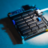
Test Detects COVID-19 in 30 Seconds
#19in30
Test Detects COVID-19 in 30 Seconds
#19in30
Co-Investigator Network
Inactive Expert
Cammy Abernathy
Dean
University of Florida
EG-ELECTRICAL / COMPUTER, College-Engineering
caber@ufl.edu
Timothy Anderson
Dist. Prof. & Director, FESC
University of Florida
EG-FESC-ADMINISTRATION, College-Engineering
tim@ufl.edu
Inactive Expert
Jean Andino
ASO PROFESSOR
University of Florida
EG-ENVIRONMENTAL, College-Engineering
Jennifer Andrew
Margaret A. Ross Associate Professor
University of Florida
EG-MATERIALS SCI ENGINEERING, College-Engineering
jandrew@mse.ufl.edu
Inactive Expert
Samim Anghaie
PROFESSOR
University of Florida
EG-NUCLEAR / RADIOLOGICAL, College-Engineering
anghaie@ufl.edu
Michael Annable
PROFESSOR
University of Florida
EG-ENG SCH SUSTAIN INFRST ENV, College-Engineering
michael.annable@essie.ufl.edu
Inactive Expert
Billy Appleton
Professor
University of Florida
EG-NIMET, College-Engineering
bappl@ufl.edu
David Arnold
Associate Professor
University of Florida
EG-ELECTRICAL / COMPUTER ENG, College-Engineering
darnold@ufl.edu
Tetsuo Ashizawa
University of Florida
MD-NEUROSCIENCE, College-Medicine
ashizawa@ufl.edu
James Baciak
Associate Professor
University of Florida
EG-MATERIALS SCIENCE, College-Engineering
jebaciak@ufl.edu
Christopher Batich
PROF
University of Florida
EG-MATERIALS SCI ENGINEERING, College-Medicine And Engineering
cbati@ufl.edu
Russell Bauer
PROFESSOR
University of Florida
HP-CLINICAL / HLTH PSYCHOLOGY, College-Publ Hlth / Hlth Profs
rbauer@phhp.ufl.edu
Adam Beck
AST PROFF
University of Florida
MD-SURGERY-VASCULAR, College-Medicine
adam.beck@surgery.ufl.edu
Inactive Expert
Howard Beck
PROFESSOR
University of Florida
AG-SCHL FOR, FISH, & GEOMATICS, College- Agricul / Nat Res
hwb@ufl.edu
Inactive Expert
Andrea Behrman
Associate Profe
University of Florida
HP-PHYSICAL THERAPY, College-Publ Hlth / Hlth Profs
abehrman@phhp.ufl.edu
Inactive Expert
Spiros Blackburn
University of Florida
MD-NEUROLOGICAL SURGERY, College-Medicine
-
David Borchelt
Professor, Director SantaFe Health Alzheimer’s Disease Research Center
University of Florida
MD-NEUROSCIENCE-GENERAL, College-Medicine
drb1@ufl.edu
Inactive Expert
Gijsbertus Bosman
PROFESSOR
University of Florida
EG-INTEGRTD PROD / PROCESS DES, College-Engineering
bosman@ece.ufl.edu
Inactive Expert
Scott Brown
University of Florida
EG-PARTICLE ENG RES CTR, College-Engineering
scottbcn@ufl.edu
Ray Bucklin
PROFESSOR
University of Florida
AG-AGRICUL / BIOLOGICAL ENG, College- Agricul / Nat Res
bucklin@ufl.edu
Jason Butler
Associate Professor
University of Florida
EG-CHEMICAL ENGINEERING, College-Engineering
butler@che.ufl.edu
Eduardo Candelario Jalil
Associate Professor, Graduate Co-Coordinator Neuroscience Graduate Program
University of Florida
MD-NEUROSCIENCE-GENERAL, College-Medicine
ecandelario@ufl.edu
Inactive Expert
Louis Cattafesta
PROFESSOR
University of Florida
EG-RES & ENG ED FAC (REEF), College-Engineering
cattafes@ufl.edu
Vijayendran Chandran
Assistant Professor
University of Florida
MD-CHILD HEALTH RES INSTITUTE, College-Medicine
vijayendran@ufl.edu
Inactive Expert
Christine Chase
PROFESSOR
University of Florida
AG-HORTICULTURAL SCIENCES, College- Agricul / Nat Res
cdchase@ufl.edu
Anuj Chauhan
AST PROFESSOR
University of Florida
EG-CHEMICAL ENGINEERING, College-Engineering
chauhan@che.ufl.edu
Inactive Expert
Ashvini Chauhan
POST DOC ASO
University of Florida
RE-VP FOR RESEARCH, Uf Research
ashvini@ufl.edu
Jacob Chung
EMINENT SCHOLAR
University of Florida
EG-MECHANICAL / AEROSPACE ENG, College-Engineering
jnchung@ufl.edu
Arthur Clark
PROFESSOR
University of Florida
DN-PROSTHODONTICS DIVISION, College-Dentistry
bclark@dental.ufl.edu
Carl Crane
PROFESSOR
University of Florida
EG-MECHANICAL / AEROSPACE ENG, College-Engineering
carl.crane@gmail.com
Inactive Expert
Bruce Crosson
PROFESSOR
University of Florida
HP-CLINICAL / HLTH PSYCHOLOGY, College-Publ Hlth / Hlth Profs
bcrosson@phhp.ufl.edu
Erica Dale
University of Florida
MD-PHYSIOLOGY AND AGING, College-Medicine
ericadale@ufl.edu
Inactive Expert
Janis Daly
University of Florida
MD - VASCULAR NEUROLOGY, College-Medicine
janisdaly@ufl.edu
Steven De Kosky
Deputy Director, McKnight Brain Institute; Aerts-Cosper Professor Of Alzheimer's Research; Associate Director 1Florida AD Research Center' And Professor Of Neurology & Neuroscience
University of Florida
MD-BEHAVIORAL NEUROLOGY, College-Medicine
steven.dekosky@neurology.ufl.edu
Inactive Expert
Donn Dennis
Emeritus Professor of Anesthesiology
University of Florida
MD-ANESTHESIOLOGY-GENERAL, College-Medicine
ddennis@anest.ufl.edu
Sylvain Dore PhD FAHA
Professor
University of Florida
MD-ANESTHESIOLOGY-GENERAL, College-Medicine
sdore@ufl.edu
Inactive Expert
Martha Douglas Escobar
Assistant Professor of Pediatrics
University of Florida
MD-PEDS-NEONATOLOGY, College-Medicine
marthave@ufl.edu
Inactive Expert
James Dyer
PROFESSOR EMERITUS
University of Florida
AG-AG ED AND COMMUNICATION, College- Agricul / Nat Res
jedyer@ufl.edu
Inactive Expert
Fereshteh Ebrahimi
PROFESSOR
University of Florida
EG-MECH AND AERO, College-Engineering
febra@mse.ufl.edu
William Eisenstadt
PROFESSOR
University of Florida
EG-ELECTRICAL / COMPUTER ENG, College-Engineering
wre@tec.ufl.edu
Josephine Esquivel-Upshaw
Professor
University of Florida
DN-PROSTHODONTICS DIVISION, College-Dentistry
jesquivel@dental.ufl.edu
Inactive Expert
Peggy Evanich
Scientist
University of Florida
LS-ASTRONOMY, College-Liberal Arts/Sciences
pegy.evanich@smallsatelliteinnovations.com
Z. Hugh Fan
Professor
University of Florida
EG-Mechanical & Aerospace Engineering, College-Engineering
hfan@ufl.edu
Inactive Expert
William Farmerie
Scientist & Associate Program Director
University of Florida
SR-ICBR-MS, Research / Sponsored Programs
wgf2@ufl.edu
Marcelo Febo Vega
Associate Professor
University of Florida
MD-PSYCHIATRY, College-Medicine
febo@ufl.edu
Robert Ferl
Distinguished Professor
University of Florida
AG-HORTICULTURAL SCIENCES, College- Agricul / Nat Res
robferl@ufl.edu
Inactive Expert
David Fitzgerald
Clinical Assistant Professor
University of Florida
HA-MBI NEUROTRAUMA RES PROG, Office Of Health Affairs
dfitzger@ufl.edu
Kevin Folta
Professor
University of Florida
AG-HORTICULTURAL SCIENCES, College- Agricul / Nat Res
kfolta@ufl.edu
David Fuller
Professor
University of Florida
HP-PHYSICAL THERAPY, College-Publ Hlth / Hlth Profs
dfuller@phhp.ufl.edu
Inactive Expert
Maria Gallo
Professor
University of Florida
AG-AGRONOMY, College- Agricul / Nat Res
gallom@ctahr.hawaii.edu
Steven Ghivizzani
Professor
University of Florida
MD-ORTHOPAEDICS / REHAB, College-Medicine
sghiv@ufl.edu
Brent Gila
Asso Engineer
University of Florida
EG-RESEARCH SERVICE CENTERS, College-Engineering
bgila@ufl.edu
Inactive Expert
Alexander Glushakov
Assistant Professor
University of Florida
MD-ANESTHESIOLOGY-GENERAL, College-Medicine
glushav@UFL.EDU
Inactive Expert
Mark Gold
Psychiatry DIZNEY EMINENT SCHOLAR & CHAIR
University of Florida
HP-BEHAVIORAL SCI COMM HLTH, College-Publ Hlth / Hlth Profs
msgold@ufl.edu
Luiz Gonzaga
Clinical Associate Professor
University of Florida
DN-IMPLANT CENTER, College-Dentistry
lgonzaga@ufl.edu
Elisa Gonzalez-Rothi
RESEARCH ASSISTANT PROFESSOR
University of Florida
HP-PHYSICAL THERAPY, College-Publ Hlth / Hlth Profs
elisagon@ufl.edu
Jing Guo
Professor
University of Florida
EG-ELECTRICAL / COMPUTER ENG, College-Engineering
guoj@ufl.edu
William Gurley
PROFESSOR
University of Florida
AG-MICROBIOLOGY / CELL SCI, College- Agricul / Nat Res
wgurley@ufl.edu
Inactive Expert
Charles Guy
Professor Emeritus and Courtesy Professor
University of Florida
AG-ENVIRONMENTAL HORTICULTURE, College- Agricul / Nat Res
clguy@ufl.edu
Helena Hagelin Weaver
ASST PROFESSOR
University of Florida
EG-CHEMICAL ENGINEERING, College-Engineering
hweaver@che.ufl.edu
David Hahn
Courtesy Professor
University of Florida
EG-MECHANICAL / AEROSPACE ENG, College-Engineering
dwhahn@ufl.edu
Larkin Hannah
PROFESSOR
University of Florida
AG-HORTICULTURAL SCIENCES, College- Agricul / Nat Res
lchannah@ufl.edu
Kyle Hartig
University of Florida
EG-MATERIALS SCI ENGINEERING, College-Engineering
kyle.hartig@ufl.edu
Kirk Hatfield
PROFESSOR
University of Florida
EG-ENG SCH SUSTAIN INFRST ENV, College-Engineering
kirk.hatfield@essie.ufl.edu
Arthur Hebard
Distinguished Professor
University of Florida
LS-PHYSICS-GENERAL, College-Liberal Arts/Sciences
afh@ufl.edu
Inactive Expert
Daniel Hoh
Associate Professor
University of Florida
MD-NEUROLOGICAL SURGERY-GEN, College-Medicine
daniel.hoh@neurosurgery.ufl.edu
Paul Holloway
DIS PROFESSOR
University of Florida
EG-MATERIALS SCI ENGINEERING, College-Engineering
pholl@mse.ufl.edu
Inactive Expert
Rolf Hummel
Pamphalon PROFESSOR - Electronic Materials
University of Florida
EG-MATERIALS SCIENCE, College-Engineering
rhumm@mse.ufl.edu
Peter Ifju
PROFESSOR
University of Florida
EG-MECHANICAL / AEROSPACE ENG, College-Engineering
ifju@ufl.edu
Gary Ihas
Professor
University of Florida
LS-PHYSICS-GENERAL, College-Liberal Arts/Sciences
ihas@phys.ufl.edu
Inactive Expert
Herbert Ingley
ASO PROFESSOR
University of Florida
EG-HINKLEY CENTER, College-Engineering
ingley@ufl.edu
Michael Jaffee
Chair and Professor of Neurology
University of Florida
MD-NEUROLOGY-ADMIN/EDUC, College-Medicine
michael.jaffee@ufl.edu
Kevin Jones
PROF & past-CHR
University of Florida
EG-MATERIALS SCI ENGINEERING, College-Engineering
kjones@eng.ufl.edu
James Klausner
Professor
University of Florida
EG-MECHANICAL / AEROSPACE ENG, College-Engineering
klaus@ufl.edu
Inactive Expert
Ben Koopman
PROFESSOR
University of Florida
EG-PARTICLE ENG RES CTR, College-Engineering
bkoop@ufl.edu
Sanjeev Koppal
University of Florida
EG-ELECTRICAL / COMPUTER ENG, College-Engineering
sjkoppal@ece.ufl.edu
Inactive Expert
James Kurtz
RESEARCH ENGINEER
University of Florida
EG-ELECTRICAL / COMPUTER, College-Engineering
jkurtz@ufl.edu
Mark Law
Prof. and Director of the Honors Pr
University of Florida
EG-MATERIALS SCI ENGINEERING, College-Engineering
mlaw@ufl.edu
Inactive Expert
William Lear
Aso Professor Emeritus
University of Florida
EG-MECHANICAL / AEROSPACE ENG, College-Engineering
lear@ufl.edu
Yoonseok Lee
Professor
University of Florida
LS-PHYSICS-GENERAL, College-Liberal Arts/Sciences
ysl@ufl.edu
Tanmay Lele
Faculty
University of Florida
MD-ANATOMY-GENERAL, College-Medicine
tlele@che.ufl.edu
Marino Leon
CLINICAL PROFESSOR
University of Florida
MD-PATHOLOGY-GENERAL, College-Medicine
marino.leon@ufl.edu
Inactive Expert
Stephen Lewis
ASSOCIATE PROFESSOR
University of Florida
MD-NEUROLOGICAL SURGERY, College-Medicine
lewissb@ufl.edu
Jenshan Lin
PROFESSOR
University of Florida
Electrical and Computer Engineering, College-Engineering
jenshan@ufl.edu
Brian Lobo
Assistant Professor, Division of Rhinology & Skull Base Surgery, Associate Chief Medical Informatics Officer UF Health
University of Florida
MD-OTOLARYNGOLOGY, College-Medicine
brian.lobo@ent.ufl.edu
Thomas Mareci
Professor
University of Florida
Biochemistry and Molecular Biology, Medicine
thmareci@ufl.edu
Charles Martin
Distinguished & Crow Professor
University of Florida
LS-CHEMISTRY-GENERAL, College-Liberal Arts/Sciences
crmartin@chem.ufl.edu
David Mazyck
PROFESSOR
University of Florida
EG-SCHOOL SUSTAIN INFRST ENVIR, College-Engineering
dmazyck@ufl.edu
Donald Mccarty
Professor
University of Florida
AG-HORTICULTURAL SCIENCES, College- Agricul / Nat Res
drm@ufl.edu
Lisa McElwee-White
Crow Professor and Chair
University of Florida
LS-CHEMISTRY-GENERAL, College-Liberal Arts/Sciences
lmwhite@chem.ufl.edu
Inactive Expert
Renwei Mei
PROFESSOR
University of Florida
EG-MECH AND AERO, College-Engineering
rwmei@ufl.edu
Inactive Expert
Alexandra Mendez Garraud
University of Florida
EG-INTEGRTD PROD & PROCESS DES, College-Engineering
agarraud@ufl.edu
Inactive Expert
David Mikolaitis
ASO PROFESSOR EMERITUS
University of Florida
EG-MECHANICAL / AEROSPACE ENG, College-Engineering
mollusk@ufl.edu
Gordon Mitchell
Professor
University of Florida
HP-PHYSICAL THERAPY, College-Publ Hlth / Hlth Profs
gsmitche@phhp.ufl.edu
Saeed Moghaddam
University of Florida
EG-MECHANICAL / AEROSPACE ENG, College-Engineering
saeedmog@ufl.edu
Timothy Morey
Professor and Chair
University of Florida
MD-ANESTHESIOLOGY-GENERAL, College-Medicine
morey@ufl.edu
Inactive Expert
Brij Moudgil
PROFESSOR
University of Florida
EG-MATERIALS SCI ENGINEERING, College-Engineering
bmoudgil@perc.ufl.edu
Inactive Expert
Khai Ngo
PROFESSOR
University of Florida
EG-ELECTRICAL / COMPUTER, College-Engineering
kdtn@ufl.edu
Wayne Nicholson
Professor
University of Florida
AG-MICROBIOLOGY / CELL SCI, College- Agricul / Nat Res
wln@ufl.edu
Juan Nino
Professor
University of Florida
EG-MATERIALS SCI ENGINEERING, College-Engineering
jnino@mse.ufl.edu
Toshikazu Nishida
PROFESSOR
University of Florida
EG-ACADEMIC PROGRAMS, College-Engineering
nishida@ufl.edu
David Norton
Vice President for Research
University of Florida
SR-VP FOR RESEARCH, College-Engineering
DPNORTON@UFL.EDU
Inactive Expert
Kenneth O
PROFESSOR
University of Florida
EG-ELECTRICAL / COMPUTER ENG, College-Engineering
kko@tec.ufl.edu
Michael Okun
ADELAIDE LACKNER ASSOCIATE PROFESSOR
University of Florida
MD-NEUROLOGY-MOVEMENT DISORDER, College-Medicine, Center For Movement Disorders And Neurorestoration
okun@neurology.ufl.edu
Mark Orazem
DISTINGUISHED PROFESSOR
University of Florida
EG-CHEMICAL ENGINEERING, College-Engineering
meo@che.ufl.edu
Inactive Expert
Edward Osborne
PROF
University of Florida
ewo@ufl.edu
Inactive Expert
Chang Park
PROFESSOR
University of Florida
EG-CHEMICAL, College-Engineering
park@che.ufl.edu
Erin Patrick
Research Assistant Professor
University of Florida
EG-ELECTRICAL / COMPUTER ENG, College-Engineering
ee1@ufl.edu
Annalisa Paul
Research Professor and Director
University of Florida
RE-ICBR-AUX&HSC, Uf Research
alp@ufl.edu
Stephen Pearton
DIS PROFESSOR
University of Florida
EG-MATERIALS SCI ENGINEERING, College-Engineering
spear@mse.ufl.edu
Inactive Expert
Jill Peterson
ASO PROFESSOR
University of Florida
EG-MECH AND AERO, College-Engineering
jepete@ufl.edu
Inactive Expert
Winfred Phillips
Executive Chief of Staff
University of Florida
ADMINISTRATION, Administration
wphil@ufl.edu
Simon Phillpot
Professor and Chair
University of Florida
EG-MATERIALS SCI ENGINEERING, College-Engineering
sphil@mse.ufl.edu
Inactive Expert
Kevin Powers
Associate Director R&D Facilities
University of Florida
EG-INTEGRTD PROD / PROCESS DES, College-Engineering
kpowers@perc.ufl.edu
Paul Reier
ANNE and OSCAR LACKNER EMINENT SCHOLAR
University of Florida
MD-NEUROSCIENCE, College-Medicine
reier@ufl.edu
Stephen Roberts
Professor and Program Director
University of Florida
VM-PHY SCI, Hsc - Veterinary Medicine
smroberts@ufl.edu
Inactive Expert
William Rossi
Clinical Professor
University of Florida
BA-FIRE BUSINESS OFFICE, College-Business Administration
rossiwj@ufl.edu
Nancy Ruzycki
University of Florida
EG-MATERIALS SCI ENGINEERING, College-Engineering
nruzycki@mse.ufl.edu
Bhavani Sankar
PROFESSOR
University of Florida
EG-MECHANICAL / AEROSPACE ENG, College-Engineering
sankar@ufl.edu
Inactive Expert
Nihal Scarpace
PROFESSOR
University of Florida
MD-PHARMACOLOGY-GENERAL, College-Medicine
ntumer@ufl.edu
Christine Schmidt
Professor and Chair
University of Florida
EG-BIOMEDICAL ENGINEERING, College-Engineering
schmidt@bme.ufl.edu
Inactive Expert
Tony Schmitz
Associate Professor
University of Florida
EG-MECH AND AERO, College-Engineering
tschmitz@ufl.edu
Andrew Schuerger
University of Florida
AG-PLANT PATHOLOGY, College- Agricul / Nat Res
schuerg@ufl.edu
Luciana Shaddox
Assistant Professor
University of Florida
DN-PERIODONTICS, College-Dentistry
lshaddox@ufl.edu
Inactive Expert
Gerry (Gerard) Shaw
PROFESSOR
University of Florida
MD-NEUROSCIENCE, College-Medicine
shaw@mbi.ufl.edu
Inactive Expert
William Sheehan
AST ENGINEER
University of Florida
RE-VP FOR RESEARCH, Uf Research
wsheehan@ees.ufl.edu
Mark Sheplak
PROFESSOR
University of Florida
EG-MECHANICAL / AEROSPACE ENG, College-Engineering
sheplak@ufl.edu
Inactive Expert
Vishnumurthy Shushrutha Hedna
Assistant Professor
University of Florida
MD - VASCULAR NEUROLOGY, Office Of Health Affairs
v.hedna@neurology.ufl.edu
Inactive Expert
Wei Shyy
PROF & CHR
University of Florida
EG-MECH AND AERO, College-Engineering
wss@mae.ufl.edu
Wolfgang Sigmund
PROFESSOR
University of Florida
EG-MATERIALS SCI ENGINEERING, College-Engineering
sigmund@ufl.edu
Susan Sinnott
PROFESSOR
University of Florida
EG-MECHANICAL / AEROSPACE ENG, College-Engineering
sinnott@ufl.edu
Christopher Stanton
Professor
University of Florida
LS-PHYSICS-GENERAL, College-Liberal Arts/Sciences
stanton@ufl.edu
Dennis Steindler
Joseph J. Bagnor/Shands Professor of Medical Research
University of Florida
MD-NEUROLOGICAL SURGERY, College-Medicine
steindler@neurosurgery.ufl.edu
Jon Stewart
Professor
University of Florida
LS-CHEMISTRY-GENERAL, College-Liberal Arts/Sciences
jds2@chem.ufl.edu
Neil Sullivan
PROFESSOR
University of Florida
LS-MAGNETIC LAB, College-Liberal Arts/Sciences
neilsull@ufl.edu
Roozbeh Tabrizian
Assistant Professor
University of Florida
EG-ELECTRICAL / COMPUTER ENG, College-Engineering
rtabrizian@ufl.edu
Weihong Tan
Distinguished & Jackson Professor
University of Florida
LS-CHEMISTRY-GENERAL, College-Liberal Arts/Sciences
tan@chem.ufl.edu
Inactive Expert
Arthur Teixeira
PROFESSOR
University of Florida
AG-AGRICUL / BIOLOGICAL ENG, College- Agricul / Nat Res
atex@ufl.edu
Inactive Expert
Floyd Thompson
Professor, Research Career Scientist
University of Florida
Brain Rehabilitation Research Center, Malcom Randal Veterans Affairs Medical Center
thompson@mbi.ufl.edu
Scott Thompson
Associate Professor
University of Florida
EG-ELECTRICAL / COMPUTER ENG, College-Engineering
cmos@ufl.edu
Michael Tonks
Associate Professor
University of Florida
EG-MATERIALS SCI ENGINEERING, College-Engineering
michael.tonks@ufl.edu
Roger Tran Son Tay
PROFESSOR
University of Florida
EG-MECHANICAL / AEROSPACE ENG, College-Engineering
rtst@ufl.edu
James Tulenko
Professor and Director, Laboratory for Development of Advanced Nuclear fuels and Materials
University of Florida
EG-NUCLEAR / RADIOLOGICAL, College-Engineering
tulenko@ufl.edu
Inactive Expert
Shahabeddin Vahdat
University of Florida
HA-MBI NEUROTRAUMA RES PROG, Office Of Health Affairs
svahdat@ufl.edu
Inactive Expert
Carlos Vallejos
ASO PROFESSOR
University of Florida
AG-HORTICULTURAL SCIENCES, College- Agricul / Nat Res
vallejos@ufl.edu
Inactive Expert
Manoj Varshney
Adj. Research Associate Scientist
University of Florida
EG-PARTICLE ENG RES CTR, College-Engineering
varshney@ufl.edu
Inactive Expert
Eric Wachsman
PROFESSOR
University of Florida
EG-FESC-ADMINISTRATION, College-Engineering
ewach@mse.ufl.edu
Aparna Wagle Shukla
Professor of Neurology Director, Clinical Trials
University of Florida
MD-NEUROLOGY-MOVEMENT DISORDER, College-Medicine
aparna.shukla@neurology.ufl.edu
Kevin Wang
Psychiatry Faculty
University of Florida
MD-PSYCHIATRY, College-Medicine
kwang@psychiatry.ufl.edu
Michael Waters
Assistant Professor
University of Florida
EG-BIOMEDICAL ENGINEERING, College-Engineering
-
Jason Weaver
PROFESSOR
University of Florida
EG-CHEMICAL ENGINEERING, College-Engineering
weaver@che.ufl.edu
Michael Weiss
Professor; Medical Director, ShandsCair Neonatal/Pediatric Transport Team
University of Florida
MD-PEDS-NEONATOLOGY, College-Medicine
mweiss@ufl.edu
Inactive Expert
Keith White
PROFESSOR EMERITUS
University of Florida
LS-PSYCHOLOGY-GENERAL, College-Liberal Arts/Sciences
kdwhite@ufl.edu
Chang-Yu Wu
PROFESSOR
University of Florida
EG-ENG SCH SUSTAIN INFRST ENV, Engineering
cywu@ufl.edu
Wenhsing Wu
Lecturer
University of Florida
EG-ELECTRICAL / COMPUTER ENG, College-Engineering
wenhsing@ufl.edu
Huikai Xie
PROFESSOR
University of Florida
EG-ELECTRICAL / COMPUTER ENG, College-Engineering
hkx@ufl.edu
Zhihui Yang
Research Assistant Professor & Associate Director NNBR
University of Florida
MD-EMERGENCY MED-AED, College-Medicine
zhihuiyang@ufl.edu
Yong Yoon
Faculty
University of Florida
EG-ELECTRICAL / COMPUTER ENG, College-Engineering
ykyoon@ece.ufl.edu
Websites
0000-0001-9234-019X
Search Google Scholar for Fan Ren
Contact Information
ren@che.ufl.edu
3523924727
1030 CENTER DR GAINESVILLE, FL 32611-2023
Profile QR code
What is this?
Keyword Search
Please enter valid search criteria.
Search
Centers
Experts
Projects
Speakers
Stories
Technologies
Videos
University
All Universities
Florida A&M University
Florida Atlantic University
Florida Gulf Coast University
Florida Institute of Technology
Florida International University
Florida State University
University of Central Florida
University of Florida
University of Miami
University of North Florida
University of South Florida
University of West Florida
Browse by STEM
Biotechnology
Computer Science
Energy
Engineering
Environmental Sciences
Information Science
Life Sciences
Mathematics
Medical Sciences
Military Sciences
Natural Sciences
Physical Sciences
Plant Sciences
Science
Space Sciences
Technology
Transportation